
Edge AI is becoming a subsystem problem. On Monday, November 9, 2026, Expedera announced a collaboration with Cadence to pair its Origin Evolution neural processing unit (NPU) with the Cadence Tensilica NeuroEdge 130 AI Co-Processor in a pre-silicon simulation, creating what the companies call a validated AI subsystem for edge inference. The goal is familiar — more performance, less power, lower latency — but the approach is worth a closer look, because it shows how edge AI chips are increasingly built from pieces that come from different companies.
The announcement matters less as a product launch than as a design pattern. Neither chip here is new: Origin Evolution debuted in May 2025, and so did the NeuroEdge 130. What is new is the two of them working together as a tested combination, so a chip designer can license the pair instead of assembling the subsystem from scratch and hoping the parts cooperate.
What Expedera and Cadence Actually Announced
According to Expedera’s official announcement and the PRNewswire release, the two companies demonstrated an AI subsystem that pairs Expedera’s customizable Origin Evolution NPU with Cadence’s Tensilica NeuroEdge 130 AI Co-Processor (AICP) in a pre-silicon simulation. The simulation shows AI workloads being distributed and executed across both IP blocks, and the combined solution is designed to improve performance and power efficiency while reducing latency, cost, and complexity in edge AI inference systems.
The companies are targeting inference designs across edge nodes, smartphones, automotive systems, and data center applications. The approach can also be extended to other Tensilica digital signal processors, so the pairing is a template as much as a single product. The two teams will be showing the work together at ICCAD-Expo 2026 in Beijing on November 19–20, with Expedera at booth F091.
One distinction matters from the start: this is a validated pre-silicon integration, not a customer-silicon benchmark. Models are running on the combined subsystem in simulation, but no combined performance, power, or latency measurements were published. The announcement supplies the design goals, not the numbers that would prove them. That is normal for semiconductor IP at this stage, but it means the claims should be read as a roadmap, not a result.
A Division of Labor Inside the AI Subsystem
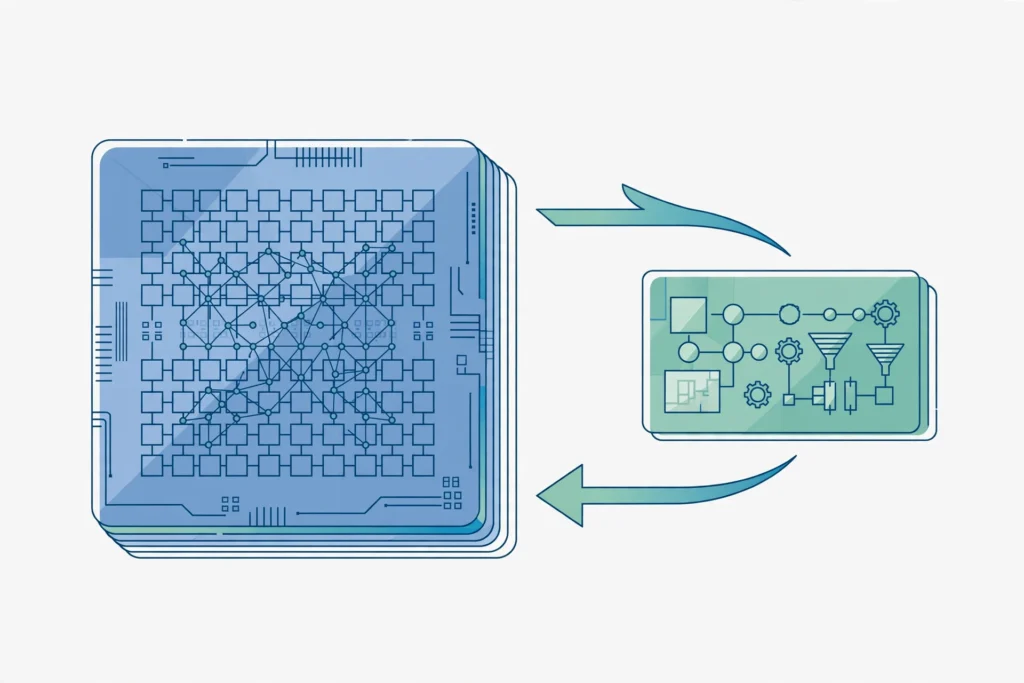
The arrangement does not assign identical work to two accelerators. Amol Borkar, group director of product management and marketing for Cadence’s Tensilica Products Group, said the NeuroEdge 130 assists Expedera’s NPU with pre-processing, post-processing, and operator fallback while also executing AI networks itself. The co-processor handles the surrounding work that NPUs are bad at, and the NPU handles the dense neural network math it was built for.
That division of labor is the whole point of the pairing. A neural network is not one uniform workload: some operations are dense matrix math, others are odd-shaped functions, data reshaping, or operators the accelerator was never designed to run. When an NPU hits an operator it cannot handle, something has to pick up the slack. In this subsystem, that something is the NeuroEdge 130, which can run those operators and keep the pipeline moving instead of bouncing the work back to a general-purpose CPU.
Cadence designed the co-processor to work alongside its own Neo NPUs, customer-developed NPUs, or third-party NPU IP. The Expedera pairing is a concrete example of that third-party route. Its product documentation describes an Xtensa-based architecture using very long instruction word (VLIW) and single instruction, multiple data (SIMD) techniques, with optimized instructions for operations such as sigmoid, tanh, and ReLU that are less suited to NPUs. The NeuroEdge 130 can also issue instructions and commands to an NPU as a control processor, adding programmability for workloads that were not anticipated when the subsystem was designed. It connects through AXI or Cadence’s High Bandwidth Direct Interface, and the NeuroWeave software development kit, built on the Tensor Virtual Machine stack, tunes, optimizes, and deploys models on Cadence AI IP.
Sharad Chole, Expedera’s chief scientist, said models are running on the combined subsystem and that agentic AI workflows are helping the company deliver customized IP more quickly. “Pairing Expedera’s packet-based NPU architecture with Cadence’s Tensilica NeuroEdge 130 AICP gives developers a validated way to add scalable, efficient AI acceleration to the workflows they already use,” he said, describing the result as “a faster, lower-risk path to production edge AI tailored to their performance and power requirements.”
How Origin Evolution’s Packet Design Fits In
Origin Evolution breaks neural networks into packets, or contiguous fragments, and routes them through Feed Forward, Attention, and Vector processing blocks. Those blocks handle different operations, data types, and precisions, while the NPU supports large language models, convolutional networks, recurrent networks, and custom or black-box layers. The packet design aims to reduce large memory movements and let different kinds of network work share one architecture.
That memory angle is central to the pitch. In edge devices, moving data to and from external memory often costs more time and energy than the actual computation. Expedera reports that Origin Evolution cuts external memory moves by more than 75% for Llama 3.2 1B and Qwen2 1.5B compared with alternative solutions, and that the NPU scales to 128 TFLOPS in a single core and to petaFLOPS and beyond with multiple cores. Those figures describe the NPU alone, not the new combined subsystem, and the same caution applies to the co-processor’s own numbers: Cadence reported more than 30% area savings and over 20% lower dynamic power and energy at comparable performance to its Tensilica Vision DSPs on AI networks and operators. Both sets of figures are real, but neither measures the Expedera-Cadence subsystem as a whole. The combined numbers are the ones still missing.
Origin Evolution debuted on May 20, 2025 as available, production-ready, and silicon-proven in customer production designs, and it was recently named Best Edge AI Processor IP in the 2026 Edge AI and Vision Product of the Year Awards. Expedera says its NPU solutions are deployed in more than 10 million consumer devices, which gives the new pairing a credibility that a brand-new accelerator would not have: the core IP has already shipped at volume.
What This Means for Phones, Cars, and Edge Devices
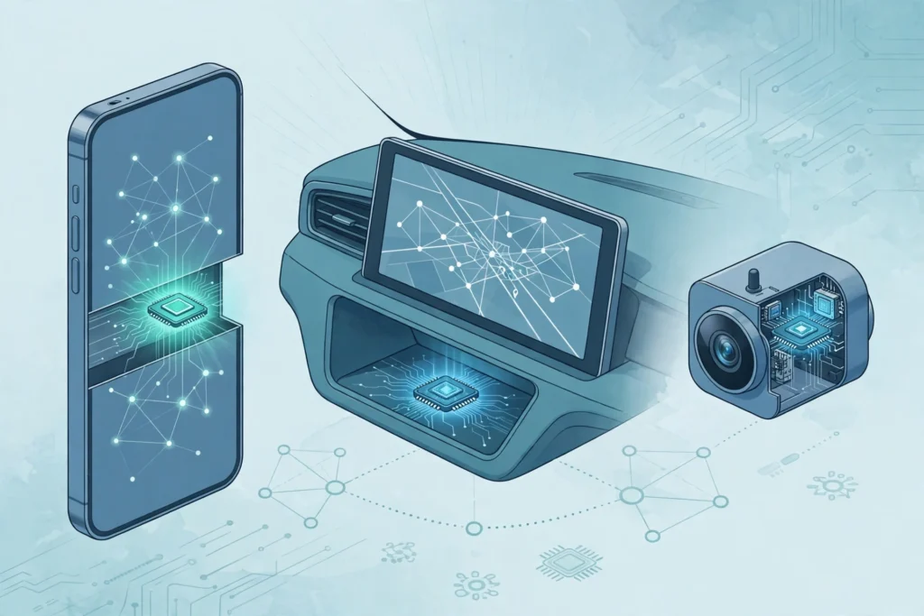
The most immediate beneficiaries of this kind of subsystem are the devices that run AI locally and cannot afford a data center’s power budget. A smartphone running a small language model on-device, a car running driver-assistance vision, or a camera doing real-time object detection all need the same thing: enough AI compute to run modern models, inside a few watts, without waiting on the cloud.
The same division-of-labor idea already ships in other edge chips. Mobilint’s REGULUS edge AI chip, announced earlier in November, pairs Ceva’s NeuPro-Nano NPU with a SensPro AI DSP to deliver 10 TOPS of on-device inference at under 3 watts. The Expedera-Cadence subsystem is the licensable-IP version of the same insight: combine a specialized neural engine with a programmable companion processor, and let each do what it does best.
For automotive designs, the co-processor’s credentials help. The NeuroEdge 130 launched with general availability and ISO 26262-ready status for automotive applications, which matters for carmakers that need functional-safety documentation before a chip can go into a vehicle. For smartphones and edge nodes, the attraction is different: a validated subsystem shortens the time between licensing IP and shipping silicon, and the companies say agentic AI workflows are speeding up the customization of that IP for each customer’s performance and power targets.
The Bigger Pattern: Modular AI Silicon
Step back, and November 9 looks like a day when the semiconductor industry kept moving in the same direction from several angles at once. NXP’s unified robotics platform, announced the same day, is built on a distributed foundation connecting sensing, real-time control, AI processing, and communication, with pre-validated interoperable subsystems that scale from individual functions to complete systems. At the data-center end of the same spectrum, Google’s new TPU 8tx and 8i Max systems split the problem differently — confidential computing on one hand, massive context windows on the other — but share the same logic of purpose-built silicon for specific AI workloads. And NVIDIA, Rebellions and SK Telecom’s sovereign AI collaboration shows the same heterogeneous thinking at rack scale, mixing NVIDIA GPUs with Korean-designed NPUs inside the same system through NVLink Fusion.
The pattern is consistent: AI hardware is no longer one chip doing everything. It is a collection of specialized blocks — NPUs, co-processors, DSPs, host CPUs — assembled into subsystems, with the interfaces and the software stack doing as much work as the silicon itself. The companies that win in edge AI may not be the ones with the fastest single accelerator, but the ones whose blocks fit together with the least friction.
That is also why the software story matters here. A subsystem is only as usable as its toolchain, and the NeuroWeave SDK is the piece that lets developers tune, optimize, and deploy models across Cadence AI IP. The risk for any modular approach is integration cost: every new block adds interfaces to verify, drivers to maintain, and edge cases where work falls between two processors. A pre-validated pairing is supposed to absorb some of that cost before the customer ever sees it. Whether it actually does will only become clear when real chips ship and real models run on them.
What to Watch Next
Three things will tell us whether this pairing matters beyond the announcement. First, whether a customer chip using the combined subsystem appears — a named design win in a phone, a car, or an edge device would turn a simulation into a product. Second, whether Expedera and Cadence publish combined measurements: real power, latency, and throughput figures for the subsystem as a whole, not the two blocks separately. And third, whether the approach extends to other Tensilica DSPs as promised, which would show this is a platform strategy rather than a one-off demonstration.
Unite.AI’s coverage makes the same point from the analyst side: for edge SoC designers, this is a validated integration path between two existing IP families, addressing the practical tension between specialized acceleration for dense network math and enough programmability to accommodate changing models. That tension is not going away. Models change faster than silicon does, and the co-processor’s job is to absorb the changes the NPU cannot. If the pairing holds up in real silicon, it gives chip designers a way to ship edge AI hardware that is both fast today and adaptable tomorrow — and that, more than any single benchmark, is what the edge AI market is actually buying.